Every distributed cryptographic protocol, key management system or wallet runs on opaque hardware. In almost all cases, we do not know with any certainty that our hardware is executing the expected program and that it is not actually acting against us. Many cases of exactly this kind of betrayal have been uncovered. The latest proved deadly. This precedent suggests the likely existence of undetected malicious hardware in use today.
In our first post, we went over the big picture security shortcomings of TEEs and broke up the work that needs to be done into two: securing the completed chip against remote and physical attackers, and securing the chip against actors in the supply chain. While there is a lot of existing work on both categories, the latter is less explored for our purposes and requires more fundamental research so we are dedicating this post to the topic, and address remote and physical attackers in the next post. A verifiable supply chain is within reach. We demonstrate this by pointing out existing and ongoing research that constitutes various pieces of the puzzle. Along the way we also cover a good deal on open hardware which will provide important context for future posts. The post is structured as follows:
- (I) making verifiable designs: if chips have embedded keys, can we tell through inspection if these keys are trustworthy?
- (II) getting a trustworthy reference: what kind of “blueprint” can we use to cross-check a chip against?
- (III) chip analysis: how do we inspect a chip to check that it is what we expect?
- (IV) making the check trustworthy for the user: the user may not be the one carrying out analysis of a chip, why should they trust a 3rd party verifier?
Parts (II) and (III) are almost universally important and touch almost every corner of computer security. The digital age is predicated on the assumption that we can safely store secrets on hardware and we are not doing the work to validate this assumption. These sections outline how we can begin to do this. The supply chain security is distinct from that provided design hiding techniques like logic locking which are used to give the chip designer - not necessarily the user - assurances that foundries are following the rules and not stealing intellectual property. These techniques can be useful in a larger design but in and of themselves do not guarantee the properties we are after.
Since our end goal is remote attestation (RA), we must also cover (I) and (IV). As a reminder, remote attesation refers to the ability to convince an arbitrary third party that a specified program is running on hardware that is controlled by an untrusted operator(s) who cannot learn about or interfere with this program. The way secure hardware (SH) achieves this is by convincing the remote verifier that the program is running on a particular piece of hardware that provides confidentiality and integrity guarantees. The supply chain issues outlined in this post are the biggest obstacle to creating a revolutionary new generation of SH.
So what are we worried about anyways?
Remote attestation and the associated cryptographic operations require a signature, which is performed with a signing key tied to the hardware. So, not only do we need to know that the hardware is doing what we expect and has the advertised security measures, we also need to be able to verify that a signature is coming from a key associated with the expected hardware.
The current chain of trust for a semiconductor looks something like the following. Note we intentionally emphasize different roles even though they are often played by the same entity.
- Design phase: A design team goes through this heavily simplified design process. The logic of the chip is dictated by the RTL (register transfer level) code -- which is just a string: a piece of code that describes the hardware in terms of the data flow between registers and the logical operations performed on that data. Writing the RTL is called the "frontend design" portion of the chip design process. The next step (the "backend design") turns that RTL into GDS, the image of the chip. Between the RTL and the GDS we find an gate-level description, the netlist. The entire process is not possible without EDA software which costs several million dollars to license and a Process Design Kit (PDK) that is provided by the fab. The PDK includes the set of building blocks (“standard cells”) required to assemble the chip image. Section (II) provides more colour on these concepts.
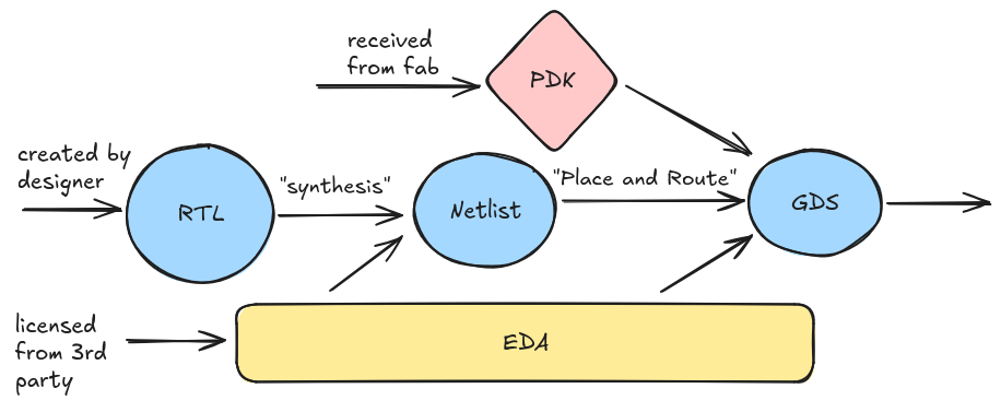
- Fabrication: The fab receives the GDS, which is pretty much a giant layered image, and prints it layer by layer. A big variable determining the performance, size and cost of the chip is the quality of the process node - the technology the fab uses to produce the chip - that is used. Big process nodes (e.g. 130nm) are less precise than smaller nodes and therefore can’t pack transistors as tightly. The state of the art is around 2nm1. Each process node has its own dedicated PDK.
- Key generation: Since the hardware needs a signing key, a key must be embedded into the hardware2. This hardware key forms part of a larger unit called the Root of Trust (RoT) that contains additional logic for using the hardware key.
- Delivery: Before being delivered to purchasers, the chip goes through several additional steps like packaging and testing. These steps may involve as many as 10 different parties gaining access to the chip. Currently, in the case of TEEs, these chips are eventually mostly sold to cloud providers.
- Generating a report: When the hardware is turned on, a boot process with the RoT at its core checks the firmware running on the device - i.e. the hardware inspects the loaded low-level software. This process produces a report about the firmware, signed by the hardware key. This signed report is sent to an attestation service which has received a database of public keys and chip metadata collected earlier in the manufacturing process.
- Attestation: If the firmware checks out and the signature matches a public key in the attestation service’s registry, the attestation service responds with a certificate confirming this.
- Verification: Now if a user wants to interact with this machine, the user can be presented with the certificate. If everything has gone to plan, this certificate shows that the hardware key indeed corresponds to a trustworthy machine.
- Building on the attestation: If we wanted to attest arbitrary applications running on the secure hardware (SH), the attested firmware can then be used to sign new software running on top of it using the hardware key or derivatives of it.
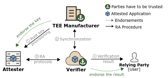
This figure taken from Teamwork makes TEE work depicts a simplified remote attestation flow.
Often several of these roles are carried out by the same actor. For example Intel is both the designer and fab for SGX and TDX (known as “integrated device manufacturing”), and also plays the role of attestation service. In other “fabless cases,” the designers and foundry are distinct. There are also often a few more keys involved, but the flow remains effectively the same.
The most obvious holes in the security of this flow are in steps 3 and 6. The user must assume the attestation service will not issue phony certificates and that no copy of the hardware key is held by entities in the supply chain who could either keep a copy if the key is injected or potentially extract the key from an unprotected chip if another key generation method is used. In both cases, the user could be mislead into believing that they are encrypting messages to a program running on secure hardware while the adversary is actually holding the decryption key in plaintext and able to run any malicious program on decrypted user data.
After concerns around the hardware key and attestation, the next category of concerns is hardware trojans. Even when the cryptographic identity system works as intended, the user is still assuming that the hardware is going to behave as advertised. Since most designs are completely closed, the user currently simply trusts that the designer isn’t adding some extra logic to leak private keys (for example) and that the fab is manufacturing hardware to the specifications provided by the designer. Attacks that do not depend on altering the hardware design or having special access to key material like side channel or direct-readout attacks, are left for a future post. However, we do consider trojans which weaken or disable defenses against such attacks.
Measuring Security
There are various models according to which we can measure security. A comprehensive analysis should incorporate all three of the following:
- Cost of attack: some attacks have measurable costs. For example, precise advanced SEM microscopes can cost hundreds of thousands of dollars and other attacks could require several months of highly skilled experts’ time. If the reward of attack approaches or exceeds the cost of attack we consider a system insecure. Once systems are implemented bounty programs in which the bounty slowly increases over time are a potential means to improve estimates of the cost of attack3.
- Difficulty of attack: some attacks have measurable difficulty. For example, we can prove that some attacks are not possible given the adversary is only able to observe d and fault k wires with each additional wire constituting a greater technical challenge (1, 2, 3). Another important metric is the number of queries an adversary needs to pull off an attack4. The ultimate goal would be to theoretically or empirically lower bound this number to be infeasibly high. Schemes built on top of SH that do not consider hardware secure after a certain life time help to make this target of “infeasibility” concrete.
- Honesty assumptions: some attacks are not possible under the assumption that certain parties behave according to a protocol. If a cloud provider is considered honest (an assumption we will not be making) then we may consider physical attacks on hardware under their control to be infeasible. At the same time, we may not consider certain supply chain actors to be honest and require a system to be secure against arbitrary actions taken by them or make statements about security conditional on k out of n actors being honest.
I. Verifiable Designs
Inevitably, building chips that don’t require strong trust assumptions in the manufacturing supply chain will require us to be able to physically inspect chips and compare them with some trustworthy reference. For this to be possible, chips that were compromised before they even get to the verification step must show physical signs of compromise. Hardware trojans are, by definition, physically embodied so we have hope of detecting them, however a compromised hardware key is not necessarily detectable. Hence, we must select a device design which generates and stores hardware keys in a manner that defends against snooping actors in the supply chain. To use academic terminology, we must use a design that avoids activatable isolation. We also need to make sure that the hardware keys cannot be extracted when used for cryptographic operations, whether through side-channel analysis, fault injection, imaging or circuit-editing attacks.
Root-of-Trust: Key Generation and Storage#
Puff, PUF, pass on key injection
We can break up our task into two: generating the key and storing it. The key must be generated so that it is unique to the device and unpredictable. We need secure storage to make the key persistent since the key acts as an identifier over the lifetime of the chip5.
A common practice is “key injection.” This features a party that generates the key externally and then stores the key within the chip by, for instance, burning it into an efuse. (e.g. Intel SGX provisioning secret). The actor generating the key is able to retain a copy of the private key, making the key predictable and the entire system insecure. Consequently, we do not consider this approach.
The first approach we do consider is using a True Random Number Generator (TRNG) on the chip to generate the key. TRNGs use the electrical noise present in the chip as a source of entropy and return ~random numbers when queried. The storage could be constructed in such a way that only the TRNG can write to it and only if all other means of reading the TRNG (e.g. for testing the TRNG) are disabled. To achieve this, the storage could be provided as an IP block that simply lacks an AXI write interface with the only wires connected to the memory storage buffers coming from the TRNG. There are several possible solutions for storing the key. A common approach is encoding the key by burning efuses. For example, Apple follows this approach for the Secure Enclave used in its consumer electronics in their recent Private Cloud Compute. However, fuses can be hard to defend against physical attackers since blown fuses are relatively large features. There are new types of memories such as resistive memories (ReRAM) or antifuses that might offer more promising alternatives. Although there are already commercial ReRAM offerings, hardware researchers have called for more thorough research to better understand their security.
The second approach we consider is a Physical Unclonable Functions (PUF) which uses manufacturing process variations as a source of entropy6. Unlike TRNGs, PUFs are designed to provide the same response over their lifetimes so the key generation occurs as a byproduct of the chip being fabricated, and the PUF itself constitutes a key-storage mechanism. The PUF derives its uniqueness and unpredictability from three important claims. The first is that no fabrication process is sufficiently precise to produce two of exactly the same chips, thus two of the same PUFs cannot be created. The second claim is that PUFs are tamper-evident. In particular, any attempt to read the fine details of the PUF so as to learn anything about the secret instantiated in its structure will disturb its structure, irreversibly destroying the key. PUFs can be constructed such that this property applies to the entire chip meaning that penetration of the passivation top layer or silicon bottom layer is not feasible as this would disturb the electrical characteristics of the chip, changing the PUF7. The third claim is that the PUF construction introduces sufficient entropy for the generated key to be secure.
For any approach, the logic that facilitates use of the key must also be secured to protect the key against attacks like side-channel and fault injection attacks. Most PUFs use error correction logic to stabilize the PUF response to ensure deterministic key generation. Signing or decryption logic must also be implemented and the key must be securely passed to this logic. State-of-the-art techniques that protect this logic make use of hardware masking to defend against side-channel attacks, and redundancy to defend against fault injection attacks.
Combining the TRNG and PUF approaches above presents the most promising design. TRNGs allow for more granular decision making over when the key is generated. If the key is only generated at verification time or when the operator receives the chip, the actors with access to the chip before that point are less of a threat. TRNGs also make verification easier since the TRNG can be sampled to check the distribution of its outputs. As a complement, the PUF adds additional tamper resistance properties and an additional key an attacker would have to compromise.
II. Getting A Trustworthy Reference
If we figure out the challenges in (I), then there should be a physical difference between a chip that was correctly produced and one that is compromised. To detect these differences, we could cross-check these chips against each other. Assuming we have the technology to detect these differences (addressed in III), the verifier need simply flag the odd ones out. But, what if all the chips have the same trojan?
Addressing this kind of attack requires us to be able to cross check a physical chip with a reference (think blueprint) that can be tied back to an auditable design, the RTL. GDS files (along with an open PDK to check that the GDS is derived from the RTL) could fill this role well, but making these accessible is no small task. To understand this challenge better, we need to take a deeper look at the hardware intellectual property (IP) landscape.
Open Hardware#
In this very insightful talk, Mark Davis makes the point that “open source” isn’t even a well-defined term in the hardware world. The legal landscape is fuzzy and there are no clear equivalents to GPL or MIT licenses. On top of this, there are various kinds of files with different roles that could be open sourced. Every phase of the design process is burdened with NDAs, tight IP-infringement monitoring and patents making opening designs a complex affair.
Usually, most of the frontend design of the chip - the RTL and netlist - can be open sourced, because it's owned by one party, however some portions such as the DRAM memory controller or clock design are often expensively licensed from a 3rd party like Cadence, Synopsys, Rambus or SiFive, and cannot legally be publicly released. The RTL is written in a high level language like VeriLog and looks something like this:
module AOI (input A, B, C, D, output F); assign F = ~((A & B) | (C & D));endmoduleThe next phase of producing the GDS file requires the netlist that we derive from the RTL, EDA software and a PDK. PDKs are provided by fabs for their process nodes and are typically kept completely closed as the PDK can reveal information about the fab processes which are core to its business. NDAs that fabs use to enforce this IP protection also extend to GDS files so fabless designers cannot release GDS files derived from these PDKs even if no 3rd party components were licensed. Old process nodes are well understood technology so some fabs open their corresponding PDK’s. The EDA software is also closed and is licensed from one of a handful of providers with the largest being Synopsys and Cadence. Given licenses for using this software cost hundreds of thousands to millions of dollars per year, the incentive for keeping the software closed is understandable. Importantly, PDKs are often certified for specific EDAs. A GDS file is pictured below.
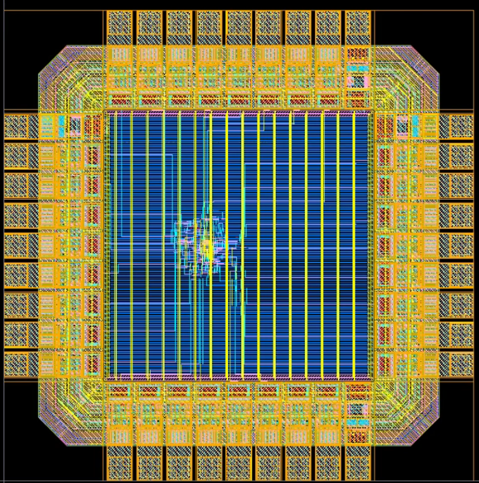
As Mark’s talk explains in more detail, there are many other files and pieces of software that sit between the designer’s idea and the GDSII file. Ownership of these is spread across a variety of parties who take legal measures to keep their IP from becoming public.
The motivation for these legal measures varies. As in the case of fabs, some actors are driven to protect advanced solutions from competitors. Security and the perception of security provides another motivation. Obscurity of design does slow attacks and open designs are more likely to draw attention from security researchers who inevitably bring bad PR. Security through obscurity has become so entrenched that the Common Criteria standard, through which almost all secure hardware is evaluated, explicitly rewards designs which are not publicly available8. At the same time, in an industry where closed designs are the norm, there has historically been limited incentive to do otherwise.
The result of this IP quagmire is that most design documentation doesn’t see the light of day. Some of the time these legal restrictions permeate all the way to low level software/firmware. For example, the critically important “microcode” that instantiates Intel’s SGX and TDX security cannot be publicly audited.
This explainer on a popular crypto hardware wallet captures the situation well:
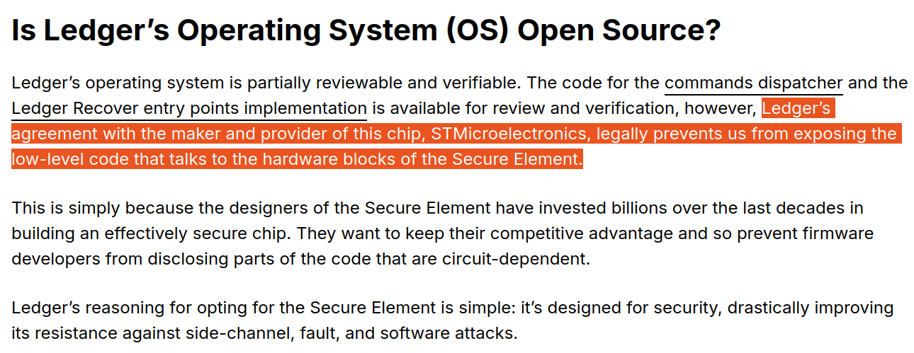
An obvious repercussion of this closedness is that, for users of these systems, there is little way to directly verify the security properties of a system without trusting private audits. An even more impactful implication is that anyone who wants to build fully open hardware, must rely on the little technology that is not legally encumbered. For components like DDR DRAM interfaces, PCIe and RISC-V cores, the closed source state of the art far outperforms open designs, impacting security and performance of open designs. This gap between closed and open technology is most critical at the level of process nodes. A determined fabless design team may be willing to implement an open source version of a needed component (at substantial cost), but this is not an option for process nodes and their PDKs. Without open PDKs, GDS files cannot be publicly released.
The fabs with open PDKs have far from the state of the art process nodes available, the most advanced being Google Skywater’s 130nm node9. Even for comparable nodes, Open PDKs have their limitations compared to closed counterparts (e.g. poor SRAM support). The quality of the process node significantly impacts the size, cost and efficiency of chips. For example, manufacturing the same chip on 28nm vs 130nm can imply a 20x cost difference and a 5-10x power/speed differential. Naturally, the difference with the 2nm state of the art is more pronounced.
Better process nodes not only imply better economics and performance, they also impact security. As chips get denser, it becomes much harder to carry out various forms of physical tampering. Extracting information via probing and electromagnetic side channel attacks becomes much more difficult for example. Interestingly, defense against hardware trojans does the inverse and becomes harder to do as features get smaller due to the limited precision of current imaging techniques. Open access to better process nodes is certainly very necessary today, but there may be a point at which smaller nodes would not be more desirable even if they were open.
How much needs to be open?#
An open source maximalist may want every design detail to be open, but given the status quo we will need to navigate a world in which not everything is open, at least for now. Despite a growing community of people and commercial projects working to build open versions of the tools required to design and build chips, there is still a very high cost to building fully open hardware, impacting the performance, cost and security of chips. There is a point at which benefits of fully open designs outweigh the costs, but significant work is required to reach this point.
Opening Everything Fortunately, there are already several designs which are partially open. OpenTitan, Cramium and Tropic Square are projects building chips with many, but not all aspects of their chip design collateral publicly released. By keeping the GDS and some other details closed, chips can be produced with high quality process nodes. However, enough material is open for users to be able to audit the design for potential bugs or side channels. For example, some side-channel mitigation techniques (1, 2, 3) can be verified by existing tooling given the netlist (1, 2, 3, 4) or RTL (1, 2). There’s also the benefit of lessened vendor lock-in and easier extensibility. To address trojans, we could throw weight behind the movement to open up tools and designs. The aim would be to get better open PDKs and make enough of an economic, social and/or political argument to sway foundries into opening up higher quality process nodes, making it possible to have a public commercially viable chip with an open GDS. Since some process nodes (e.g. ~28nm10) have been around for quite some time, the “edge” lost from opening these PDKs is not that large and it is realistic to expect that, especially with demonstration of sufficient demand, some of these will be opened up in the next 2 years.

Partial Openness#
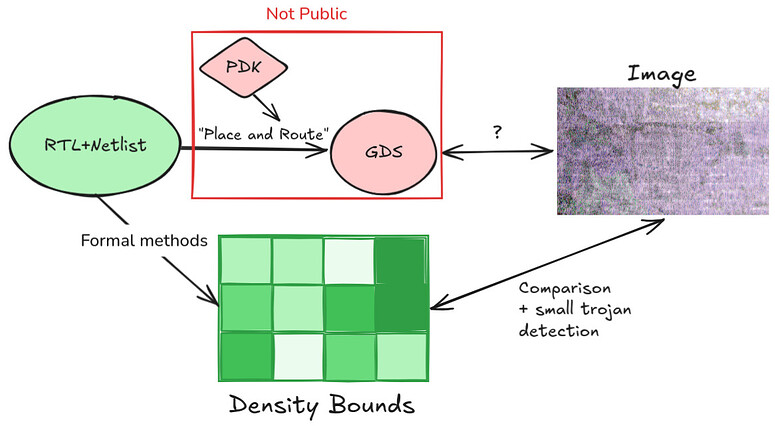
Another approach recognises that the march to a sufficiently powerful open hardware “stack” is a long and unpredictable one, and instead asks what we can do without opening everything up. The idea is to go as far as possible with only the RTL and netlist being public, using mathematical tooling to learn as much as possible from the information that is open.

One way (proposed by Bunnie) to do this is to bound the density of logic (i.e. number of transistors per unit of area) we should expect in different regions of the chip. We could rely on formal methods to achieve these bounds, but partial reliance on heuristics may also be a viable path. The reasoning behind these heuristics would be that there are large financial incentives to develop techniques to pack logic more tightly and to advertise such improvements instead of secretly developing them for the insertion of trojans. Sufficiently tight bounds would render large trojans detectable. Given how small some (dopant-level) trojans can be, we would also need other techniques to force trojans to a detectable size. We cover this issue in more depth in the next section. The proof techniques for upper bounding logic density and lower bounding trojans still need to be developed so this should be considered a direction for exploration rather than an option today11.
Other ideas require the fab to select special actors to be given access to the GDS and PDK. These chosen verifiers can use the GDS and PDK to make public statements that link an image of a chip to the netlist. These statements would actually consist of two claims:
- The verifier is in possession of a GDS and PDK such that
GDS==PlaceRoute(netlist, PDK) - The verifier is in possession of an image such that
compare(image, GDS) == truewherecompareis a public algorithm
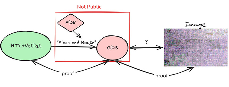
There are several techniques we can use to do this. The most basic is simply to use a quorum of actors who are trusted by the fab with access to the GDS and PDK. The fab selecting the committee of verifiers would limit how much we can trust this quorum, but it would certainly still be an improvement over the status quo. As long as one committee member is honest, we should be able to bootstrap this image. SNARKs would provide much stronger guarantees, but the feasibility of these would depend on the complexity of the (open source) comparison and layout-versus-schematic (LVS) algorithms employed as SNARKs introduce high computational overhead. Fortunately, we only need to construct a few such proofs, after which the images for which the proofs were constructed can be used to cross check other chips. A more efficient approach is to use TEEs to produce these proofs. Due to their currently limited security model, this would look something like the first idea of trusting a committee but with some additional security introduced. All of the approaches above are limited by the fab's appetite for their chips to be imaged in the first place. If a fab does not want GDS's to be public, they probably don't want images that provably resemble the GDS to be public. Design teams could be denied access to high quality process nodes if TSMC, Samsung and similar get wind of such proof generation.
The combination of the mathematical and pro-openness approaches is promising. The mathematical approaches serve as a good hedge against the open hardware movement taking a long time to get up to speed and helps to add additional assurances to partially open architectures like OpenTitan. One approach is technical while the other requires navigating patents and licensing or convincing large corporations to change their stance on something, presenting two very different forms of risk.
III. Detecting Trojans
We can separate trojan detection techniques into destructive and non-destructive. Destructive analyses are the state of the art. The destructive analysis process typically involves shaving away protective packaging and then, because chips actually consist of many layers of logic and interconnects, carefully shaving away each layer of logic and using a tool like a scanning electron microscope (SEM) or Focused Ion Beam (FIB)12 to inspect each layer. These techniques have been shown to be able to detect even stealthy dopant-level of trojans.
Despite their effectiveness, destructive techniques have significant downsides such as being, well, destructive… Not only are destructive techniques slow and costly, chips that end up being used have never gone through such an inspection process so the security guarantee must be derived from the adversary being statistically warded off by a sampling process which checks some fraction of produced chips. Additionally, as section IV makes clearer, creating publicly verifiable trojan-detection protocols based on destructive analysis is challenging because a chip can only be inspected once and the process doesn’t produce evidence that can be tied back to the identity of the chip. These limitations do not rule out the use of destructive techniques, but do motivate exploration of non-destructive alternatives.
Non-destructive approaches are intuitively more appealing, but are not nearly as developed. The most advanced non-destructive technique for analysis is x-ray ptychometry, which does a great job of imaging chips but is prohibitively expensive and requires a machine the size of a building. Due to concerns about the scalability of the approach, we leave aside x-rays. We do however include a cool video of X-ray-based 3D rendering on a chip
Fortunately, there is another promising non-destructive technique that does scale, Infra-Red In-Situ (IRIS). This technique uses short-wave infra-red light to image a chip. The infra red light can pass through silicon, but not metal, providing us with an image of the empty metal fill pattern on metal layer 1 (M1). In other words, IRIS can show us where the transistors are not, but it can’t show us what the towers of transistors do look like, nor can we learn about the wiring that connects the transistors in the deeper metal layers.
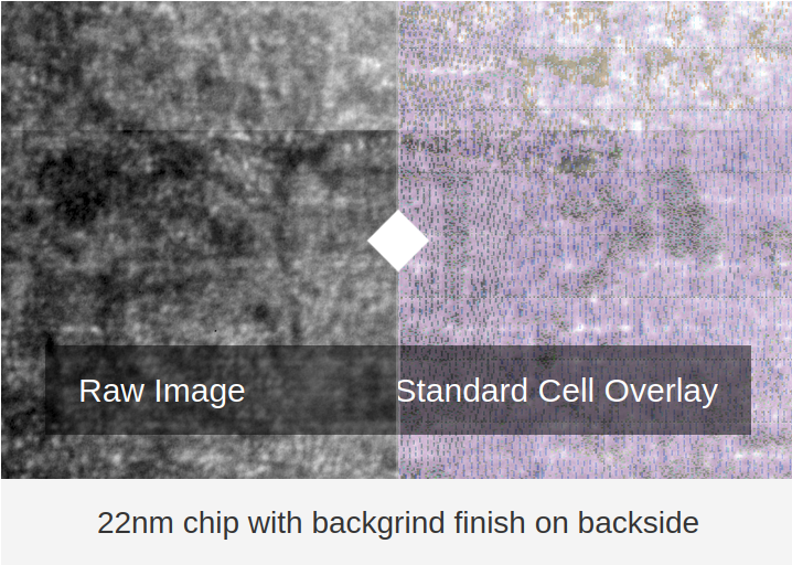 This low-resolution imaging means that IRIS is in a similar position as the mathematical proving approach outlined in (II). Since IRIS can only detect big deviations in transistor density, we must develop techniques that mitigate small trojans - i.e. trojans that do not require many additional transistors. Fortunately, there are many candidate solutions which can be used in concert. The first “solution" is black box testing like fuzzing or test vector leakage assessment (TVLA) with power analysis which can likely detect untriggered trojans that are “always on.” With sufficiently effective black box testing, we are left with triggered trojans - e.g. trojans that only take effect if a predetermined value appears on a bus. Given that a 64-bit comparison against a constant value already requires more than 100 CMOS logic gates (>400 transistors), triggered trojans may be large enough for IRIS to detect.
A similar partial solution is scan chains which logically stimulate the chip’s logic to see if the behaviour is as expected. Scan chains can be circumvented by trojans, but it may be possible to use formal methods to prove a lower bound on the size of trojans that can do so. Notably, using scan chains requires changes to the chip design. Other design choices like redundant coding schemes, sharding computations with error checking and modular redundancy are all ways to spread the footprint of a computation over a larger set of gates, so an adversary must also make their Trojans larger to attack the circuit successfully. Another example is how one picks the coding of state machine states - e.g., a one-hot encoded state machine creates roughly 2^n unused states that an attacker can hide information inside; finding ways to robustly defeat the repurposing of unused state will complicate Trojans trying to scavenge latent state space to hide from physical inspection.
Trojans which attempt to insert side channels (e.g. timing or power) may not directly be detectable by IRIS. However, checks for trojans of this nature can be built in by installing circuitry that checks for such channels and by using the infra red image to verify the correctness of this circuitry. For example, to mitigate against trojans that change the timing of processor instructions one could require that operations require a known number of clock cycles to complete, and then introduce a timer that measures the time elapsed between enable and completion. If the completion time does not match the expected time, an error is flagged. TVLA may also be an option for detecting timing channels in well-formalised algorithms. Perhaps the most challenging trojans to detect using IRIS would be changes to dopant levels or oxide masks intended to reduce PUF entropy.
Understanding the how IRIS performs on chips from smaller process nodes, developing techniques for provably lower-bounding trojan size, identifying classes of trojan attacks which are able to circumvent infra-red imaging, and designing around these slippery trojans are top open research directions. We elaborate on open questions at the end of the post.
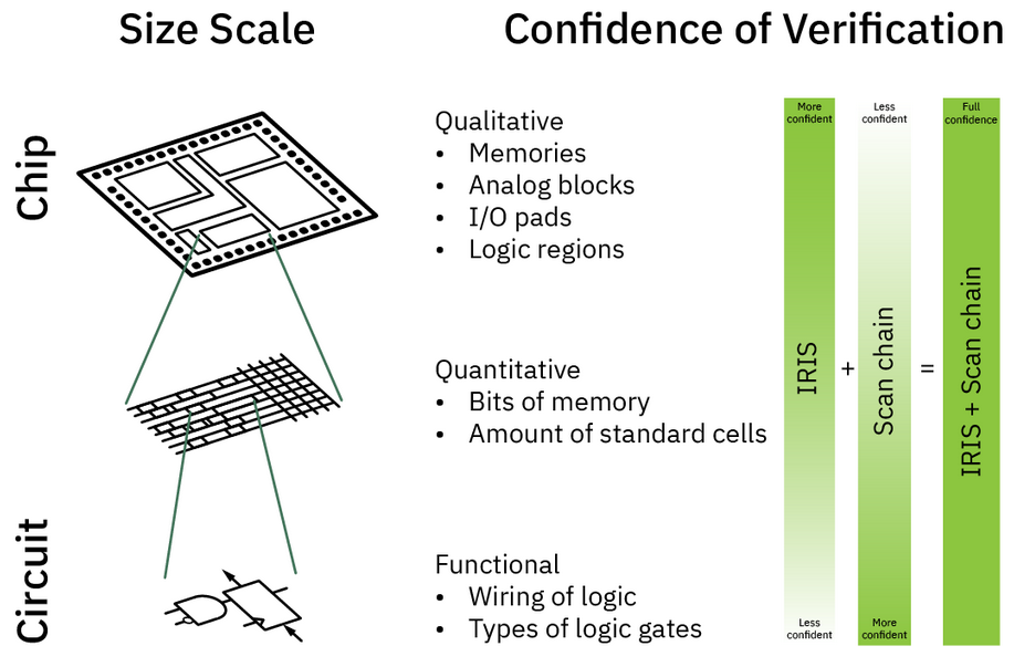 A diagram from Bunnie’s blog
Another important caveat is that designing a chip to be amenable to IRIS may be in tension with securing against physical attacks. For instance, the use of scan chains increases side channel attack surface area. IRIS also currently requires the backside of a chip to be exposed, ruling out common anti-tamper techniques like tamper-evident meshes or epoxy coatings, although detecting disturbances to backside silicon (e.g. some PUFs) remains a viable anti-temper mechanism that is compatible with IRIS. In the case where the verifier and the user are the ~same entity (e.g. hardware wallet), this is not a big complication as the verifier can apply tamper defenses like dropping epoxy on the chip “at home.” For more sophisticated users, installing tamper-evident meshes could be stronger option (we discuss tamper defenses in greater length in the next post). However, when publicly verifiable remote attestation is necessary, relying on defenses that can only be applied after inspection significantly complicates the verification process as a the next section explores.
If you want more detail, the IRIS paper gives a good overview of different detection methodologies and the update on Bunnie’s blog gives more details on the imaging itself.
IV. Decentralised Attestation Services#
Since our goal is remote attestation, we must bridge the gap between verifier and user. There is an argument that merely the threat of detection is enough to ward off most trojans given the massive reputational cost this would impose, but we take this form of guarantee as insufficient. In this section, we define a simple protocol to illustrate how a working trojan detection methodology can be used to provide the end user with trojan-freeness assurances. We intend for this protocol to spark future research that improves on the protocol and adapts it as designs and analysis techniques emerge. For cases that do not require RA, this section is not needed as long as the verification technique is cheap and easy enough to do “at home.”
Our end goal is to come up with something that allows the user to base their belief that an attestation corresponds to the expected SH on weaker assumptions than simply assuming the honesty of a large corporation. We assume a non-destructive verification mechanism that can image chips which already have tamper resistance mechanisms in place and that these mechanisms hold. All units of SH are identified by the public key which corresponds to the unit’s hardware key. We further assume that there is some governance committee that can oversee this transparent process.
- Registration: at the start of a run of the protocol that processes a bunch of chips, several forms of registration are required.
- Whomever is selling the hardware is required to register new units in a registry on a publicly verifiable blockchain.
- Entities who wish to act as verifiers also register on a publicly verifiable registry, perhaps also committing an economic bond or requiring acceptance from the governance committee.
- Entities who wish to purchase a unit must also register this intention to purchase in a publicly verifiable registry.
- Random Assignment of Verifiers: A secure source of randomness is used to assign chips to verifiers. If its not feasible to verify all chips then we sample a fraction. This means a manufacturer implanting trojans cannot anticipate which chips will be analysed or whether a verifier with whom they are in cahoots will be assigned to verifying a chip. Sellers send the chips to the verifiers who verify the chips.
- Verification: Verifiers do their checks and post signed reports (of both passes and failures) to a public registry
- For any chips that were reported to have a trojan or to be defective, a second verifier is sampled to corroborate this claim and a governance mechanism is envoked. We leave defining the governance mechanism as future work. This case should be triggered very infrequently.
- Chips that were reported to be problem-free are randomly sampled. The chips that are selected are returned to step 2, otherwise they continue to step 4. We do this sampling to disincentivise verifiers from misbehaving or lazily not checking chips.
- Random Assignment to Purchasers: Chips are randomly assigned to registered buyers from step 1. The intention behind this step is to prevent manufacturers from planting a trojan in a specific unit which would allow them to target a particular use case and minimise the probability of being detected via sampling. Even if a malicious purchaser was trying to, they could not single out the compromised hardware. When the end user requests an attestation, the hardware key is used to sign a report. The remote user can cross check this signature with the public registry of verified keys.
Depending on the selection of parameters, an analysis of this protocol could arrive at a statement like the following. Given a supply chain adversary that has a cost C if they are caught inserting a trojan and given X% honest verifiers, attempting an attack is not rational for the attacker up to a reward of successful attack of R. More complex analyses should consider rational verifiers or models in which users have heterogeneous trust assumptions across verifiers.
The protocol introduces randomness to limit the loss of security incurred in the presence of collusion between verifiers, purchasers and manufacturers, but this isn’t enough on its own. The security of the protocol also depends on how the set of verifiers is selected and what incentive schemes are constructed for the role. Ideally the set is geographically diverse and samples from actors with a variety of interests (academic institutions, NGOs, for-profit companies, etc). We could also extend the protocol to allow whistleblowers to put down collateral and nominate specific units for testing or opt out of the randomised allocation to test a specific chip themselves. Another extension could be to intentionally insert chips which should fail inspection into the pipeline (while making a commitment to their pubkeys ahead of time) as an additional countermeasure against lazy verifiers. For more on collusion, check out Vitalik’s article on the topic.
One critical assumption we made for this protocol is that we have non-destructive analysis techniques available. The problem that we ran into trying to avoid this assumption is that destructive analysis doesn’t allow the verifier to produce evidence to corroborate their claims. Yes, they can produce SEM or FIB images, but how do we tie these to a specific chip? We would want to avoid a scenario in which a manufacturer can be framed. Perhaps its sufficient to claim that such images would be hard to fake because our microscopes can do remote attestation. If there is only one designer and foundry with access to the GDS, we can attribute the trojans to these actors more readily. On the other hand, we would like a scenario in which multiple foundries were able to participate and we haven’t investigated the difficulty of faking a trojan much.
Another assumption we made is that tamper resistance mechanisms can be in place when verification happens. If this is not the case, tamper resistance mechanisms must be applied after the inspection of the IC. Simply reusing the protocol above and requiring the verifier to apply the tamper resistant measures after verifying the chip doesn’t work because then the next verifier can only check that the tamper resistance measure are in place but not that the chip was indeed trojan free. Potential improvements involve randomly deciding whether a chip will be passed to another verifier without its protection or with it or adding additional destructive sampling.
Continuous Attestation#
There are ways to extend remote attestation to defend against key extraction attacks. Some forms of attacks take several hours and damage - likely destroy - the chip from which the secrets are extracted. For any such attacks, we can leverage continuous testing to notice when a key has been extracted.
The first idea is to use a randomness beacon to generate random challenges for registered SH. The expectation is that the SH must post the signed challenge to a public blockchain within some time window. If the frequency of challenges is sufficiently high (e.g. a few hours to a few minutes), key extraction attacks should result in missed challenges. Naturally, there may be honest missed challenges due to network outages or similar failures. We will leave it up to users or protocols to decide how suspiciously to treat downtime. The second idea is to repeat the verification protocol at a certain frequency (e.g. every few months) for a randomly sampled set of chips. This should reveal attacks which physically altered chips and dissuade these kinds of attacks in the first place.
Neither of these approaches give watertight guarantees so we view continuous attestation as one more tool in the toolkit as opposed to a panacea. Attacks could happen after a chip has been inspected, before the key is registered for the uptime-challenge protocol. A hardware trojan could also make this kind of attack much faster to execute so we are relying on our detection methods being sufficiently thorough. Side-channel and fault-injection attacks which don’t need to take a chip offline clearly are unhampered by this technique and may even be aided since the critical hardware key is frequently used. Fortunately, we have theoretical foundations on which to build confidence against these kinds of attacks, especially for protecting the hardware key (more detail in the next post) and the frequency of required attestations can be controlled to tradeoff defense against active vs passive attackers.
The next post will look at attacks on complete chips in more detail.
Where does this leave us?
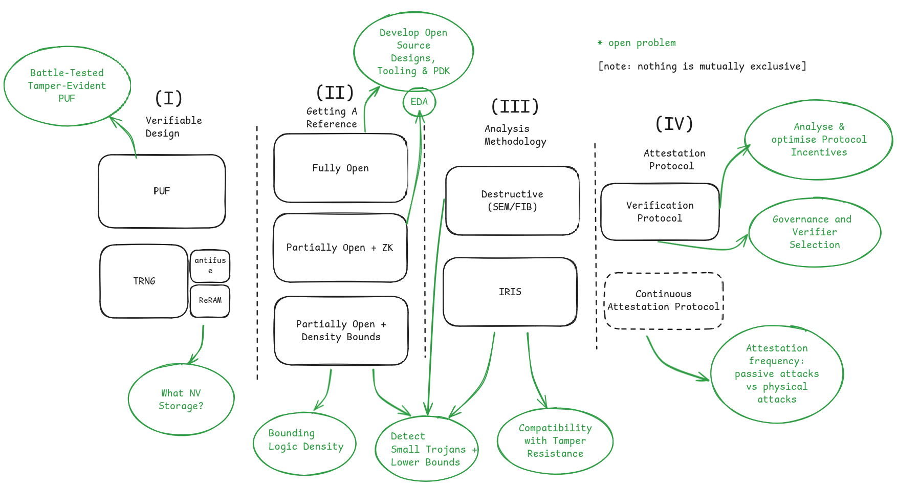
We believe the techniques described above illustrate that a supply chain with far better trust assumptions is within reach. Our writing should not be taken as an exhaustive survey - there may be much better techniques for achieving the same goals. If your favourite or newly invented approach is better, please let us know.
We have also touched on several open problems and challenges, which would be a great we to get involved. Stated at a high level:
- Root-of-Trust
- RoT security for both PUFs and TRNGs+NVM rely on assumptions that some physical task is hard to carry out. The only way of truly building confidence in these assumptions is by rigorously testing implementations. In order to do this as best as possible, we need fully open implementations and teams conducting the necessary testing.
- What is the optimal storage method for keys generated by a TRNG?
- Open source
- the tools required to make high quality and fully verifiable hardware are not yet available. This includes high quality PDKs for advanced process nodes and many system components. We can address this by:
- making a compelling case to IP owners to release their software
- developing the IP ourselves
- there are very few open reference implementations of SH.
- the tools required to make high quality and fully verifiable hardware are not yet available. This includes high quality PDKs for advanced process nodes and many system components. We can address this by:
- Formal proofs
- How tightly can we bound the logic population density? What other properties can we prove given an RTL or other easily-open-sourced design collateral?
- How large can we make a lower bound on trojan size given scan chains, design principles or other techniques?
- IRIS
- How do we have both resistance to physical attackers and allow for infra red imaging?
- Can we find a PUF design that is also amenable to IRIS verification?
- How do we detect timing and small channels?
- Remote Attestation Protocol
- Analyse, test and iterate on the simple protocol proposed, adapting to developments in trojan analysis technology and chip design.
- Design governance mechanism and consider how verifier selection should be conducted.
- For continuous attestation, understand the impact of frequency of attestations on passive side-channel attacks and physical attacks. Higher frequency should make physical attacks harder and side-channel attacks easier.
This post would not have been possible without Thorben Moos from Simple Crypto. Thanks to Zach Belateche, Leonardo Arias, James Ball and Nikki Sigurdson for valuable review and discussion.
- The actual physical pitch of features at 2nm is 45nm for gates and 20nm for metal.↩
- It is technically possible to use a software-based key, but this is worse for our purposes as will soon become clear.↩
- This could be done quite easily by passing a private key that controls some cryptocurrency to any hardware that provides a certain attestation.↩
- The cited metrics are used to measure attacks on complete chips, which is not the topic of this post. These metrics are still relevant as some trojans could be inserted to introduce side channels, but the development of other metrics would also be necessary.↩
- One could imagine protocols in which chips are reinspected and issued new identities, but we leave this aside for now.↩
- Note that there is a large body of literature about exploiting strong PUFs. These should not be conflated with the more easily realised weak PUFs we need for our use case.↩
- Delay-based PUFs are more appealing than the common SRAM PUFs as they are more resistant to invasive attacks.↩
- To reach CC-EAL-5+, a developer needs to satisfy ALC_DVS.2, which requires security controls to “protect the confidentiality and integrity of the TOE design.”↩
- 90nm may soon be on the horizon.↩
- The 2x node is also the “last node of Moore’s law” in that it was the last node where transistors got cheaper. It used to be that the cost of wafers always dropped to around $3k as the process matured; 2x nm was the end of that. For smaller nodes, wafer cost doesn’t come down, and they may even go up. This makes 2x nm a very economically important node. For instance, TSMC is doubling down on this node and trying to get legacy customers to migrate to the node.↩
- If you are knowledgeable or interested in working on (or funding) these problems reach out to us or Bunnie directly.↩
- Not to be confused with ion cannons.↩